 |
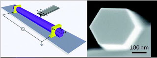
| GaN nanowires (nano letters) |
During this time people assume that the diameter of 100 nanometers is considered as one dimensional. so that analyzing one-dimensional quantum mechanics approach can be applied easily. However, recent research from Northwestern University proved it's not entirely true.
“Although nanowires are one-dimensional nanostructures, some properties – such as piezoelectricity, the linear form of electro-mechanical coupling – are three-dimensional in nature,” Espinosa said. “We thought these nanowires should show piezoelectricity in 3D, and aimed at obtaining all the piezoelectric constants for individual nanowires, similar to the bulk material.”
The study was led by Horacio Espinosa, James N. and Nancy J. Farley Professor in Manufacturing and Entrepreneurship at the McCormick School of Engineering and Applied Science, were published online Dec. 22 in Nano Letters. They use individual gallium nitride nanowires (NWS). Semiconductor GaN NWs are promising components in next generation nano- and optoelectronic systems. In addition to their direct band gap, they exhibit piezoelectricity, which renders them particularly attractive in energy harvesting applications for self-powered devices. Nanowires are often considered as one-dimensional nanostructures; however, the electromechanical coupling leads to a third rank tensor that for wurtzite crystals (GaN NWs) possesses three independent coefficients, d33, d13, and d15. Therefore, the full piezoelectric characterization of individual GaN NWs requires application of electric fields in different directions and measurements of associated displacements on the order of several picometers.
They apply an experimental approach based on scanning probe microscopy to directly quantify the three-dimensional piezoelectric response of individual GaN NWs. Experimental results reveal that GaN NWs exhibit strong piezoelectricity in three dimensions, with up to six times the effect in bulk. Based on finite element modeling, this finding has major implication on the design of energy harvesting systems exhibiting unprecedented levels of power density production. The presented method is applicable to other piezoelectric NW materials as well as wires manufactured along different crystallographic orientations.
“The measurements were very challenging, since we needed to accurately measure displacements 100 times smaller than the size of the hydrogen atom,” said Majid Minary, a postdoctoral fellow and the lead author of the study.
Source story : http://www.mccormick.northwestern.edu/news/articles/article_1025.html
Source journal : http://pubs.acs.org/doi/abs/10.1021/nl204043y
Post a Comment